
Atom chips for quantum information
Atom chips for quantum information
Neutral atom systems are a powerful platform to perform experiments at the quantum limit. Perhaps the most practically used demonstration are atomic clocks, which determine the standard of the second, determined as a fixed number of Rabi oscillations between hyperfine states of atoms such as Cesium or Rubidium, in the microwave range. The next generation of clocks aim to reach a stability in the region of 10-18, which use optical manipulations rather than microwave frequencies [1]. Other applications of ensembles include performing quantum metrology applications, which constitute precision measurements at and below standard quantum limits. Several applications of atomic ensembles include measurements of magnetic fields, rotations via Sagnac interferometry, accelerometers, and gravitational wave detection [2-5]. Neutral atom systems are also of interest for performing simulations of quantum many-body systems, fundamental quantum information experiments, and quantum computing.
One of the practical difficulties with using such atomic ensembles is the size of the system that is required. A typical setup consists of the order of a room of the order of several ~10m2. In many applications, portability is a strict requirement and important for widespread use. The next generation of clocks require development of simultaneously high stability and a portable package, of the order of several liters or less. Precision sensing of magnetic fields, and motion (acceleration/rotation) are also mainly of interest such that they can be taken out of the laboratory to on-site locations.
Atom chips have been developed to realize cold atom experiments in a compact configuration [2]. Many of the required components of a cold atom experiment, such as trapping and manipulation of the ensembles can be now be incorporated onto the chip. Figure 1 shows some examples of an atom chip. In a typical chip there is a Z-shaped wire patterned on the surface to produce a magnetic field to trap the atoms. Furthermore, microwave waveguides are present to manipulate the internal states of the atoms. Such atom chips have been used to realize Bose-Einstein condensates, and have been successfully coherently controlled using state-dependent forces [3]. They have also been successfully quantum mechanically squeezed, opening the door for quantum metrology applications [4]. Another advantage of the chip configuration is that it is intrinsically scalable, meaning that many ensembles can be placed on the same chip. This offers possibilities of performing quantum metrology with spatial resolution, allowing for example to map out magnetic field profiles. Another possibility is to enhance quantum metrology by exploiting entanglement between several ensembles [5].
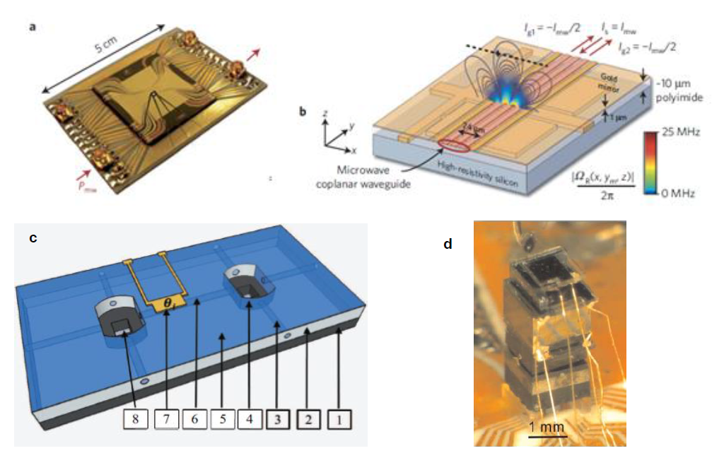
Figure 1: Examples of various atom chips. (a) photograph of atom chip for magnetic trapping with coplanar waveguides for coherent control of the atoms from Ref. [3]; (b) schematic structure showing the microwave fields generated by the waveguides [3]; (c) A schematic of an optically based atom chip as proposed in Ref. [6]; (d) All-optical chip scale atomic clock from NIST group containing the laser, optics, resonance cell with alkali vapor, and photodetector [11].
We are in collaboration with the State Key Laboratory of Precision Spectroscopy at East China Normal University developing atom chips to be used for various quantum information tasks. One of the key ideas is to perform some of the theory ideas developed here in the lab. Such coherent manipulation of two component BEC qubits have been realized on atom chip systems. In Refs. [4] arbitrary manipulation of single BEC qubits have been achieved, with arbitrary control of the state on the Bloch sphere. Furthermore, such BEC qubits have also been put into a strong coupling regime with a cavity in Ref. [5], showing that communication via cavity QED methods between qubits is also within experimental reach. Currently the primary application of such two component BECs is viewed in the community to be towards quantum metrology, as outlined in Ref. [6]. However, we believe that such BECs have possibilities that extend beyond such applications.
References
[1] A. D. Ludlow et al. “Optical atomic clocks” Rev. Mod. Phys. 87, 637 (2015).
[2] J. Riechel and V. Vuletic, “Atom chips” (Wiley, 2011).
[3] P. Böhi et al. “Coherent manipulation of Bose–Einstein condensates with state-dependent microwave potentials on an atom chip” Nature Phys. 5, 592 (2009).
[4] M. F. Riedel et al. “Atom-chip-based generation of entanglement for quantum metrology “ Nature 464, 1170 (2010).
[5] P. Anisimov et al. “Quantum Metrology with Two-Mode Squeezed Vacuum:Parity Detection Beats the Heisenberg Limit” Phys. Rev. Lett. 104, 103602 (2010).
[6] A. Abdelrahman, T. Mukai, H. Haffner and T. Byrnes, “Coherent all-optical control of ultracold atom arrays in permanent magnetic traps”, Optics Express 22, 3501 (2014).